|
| |
nextnano3 - Tutorial
1D Tutorial
Simple quantum cascade structure
-> 1DQCL_simple_nn3.in / *nnp.in
-
input file for the nextnano3 and nextnano++ software
Simple quantum cascade structure - Results
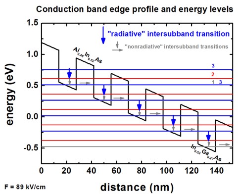
This tutorial is based on the quantum-cascade structure (Figures 12 (b) and
16 (b)) that has been presented in the following paper:
Resonant Tunneling Through Double Barriers, Perpendicular Quantum
Transport Phenomena in Superlattices, and Their Device Applications
F. Capasso, K. Mohammed, A.Y. Cho
IEEE Journal of Quantum Electronics QE-22 (9), 1853 (1986)
The following picture is based on Fig. 3 of
Simulation of quantum cascade lasers - optimizing laser performance (in
English)
S. Birner, T. Kubis, P. Vogl
Photonik international 2, 60 (2008)
Simulation zur Optimierung von Quantenkaskadenlasern
(in German)
S. Birner, T. Kubis, P. Vogl
Photonik 1, 44 (2008)
It shows the conduction band edge profile of an Al0.48In0.52As/In0.53Ga0.47As
superlattice at an electric field of -89 kV/cm.
The single-band effective-mass Schrödinger equation is solved for this band
profile.
The wave functions (psi²) of this quantum cascade structure are shown.
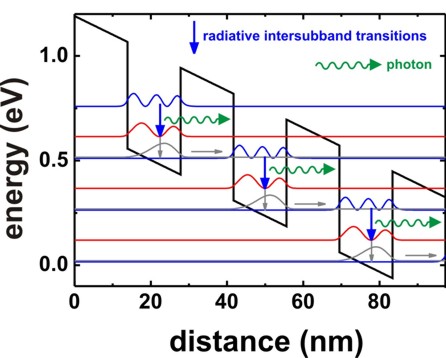
The basic idea of such a structure is to depopulate the
lowest eigenstate of each quantum well
efficiently by bringing it into resonance with the
third eigenstate of the next quantum well (resonant tunneling).
The transition second eigenstate ->
lowest eigenstate should be a nonradiative
intersubband transition whereas
the transition third eigenstate ->
second eigenstate should be a radiative
intersubband transition, i.e. a photon is emitted.
Another important condition for a quantum cascade laser is population
inversion,
i.e. the occupation of the third eigenstate
must be much higher than the occupation of the second
eigenstate and lowest eigenstate.
- The input file "
1DQCL_simple.in" should be rather intuitive
and self-explanatory.
Documentation for each keyword and each specifier can be found here:
keywords
- An example of a keyword (
$electric-field)
and a specifier (electric-field-strength) is the electric
field.
The electric field is set to -89 kV/cm.
 $electric-field

  ...

  electric-field-strength = -89d5 !
in
units of [V/m] - Here: -89 kV/cm (d5
= 105, i.e. -89 * 105 [V/m])
Output
The output files are ASCII files and can be plotted with software like e.g.
Origin.
- The conduction band edge can be found in the following file:
band_profile/cb_Gamma.dat
1st column: grid points in units of [nm]
2nd column: Gamma conduction band edge in units of [eV]
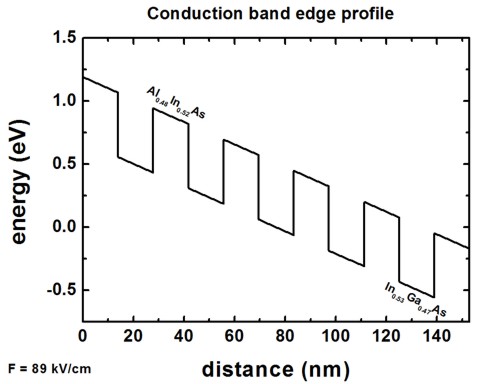
There are six Al0.48In0.52As barriers and five In0.53Ga0.47As
barriers.
The conduction band offset is 0.51 eV.
- The 40 eigenvalues that were calculated can be found in this file:
wavefunctions/ev_cb1_sg1_deg1.dat
The units are [eV].
wavefunctions/cb1_qc1_sg1_deg1_psi_squared_shift.dat
1st column: grid
points in units of [nm]
2nd column: 1st
eigenvalue in units of [eV]
- The square of the wave functions (psi²) of the 40 eigenstates can be
found in this file
wavefunctions/cb1_qc1_sg1_deg1_psi_squared_shift.dat
1st column: grid
points in units of [nm]
...
psi²n' = psi²n + En
The transition 2 ->
1 should be a nonradiative intersubband
transition whereas
the transition 3 ->
2 should be a radiative intersubband
transition, i.e. a photon is emitted.
Another important condition for a quantum cascade laser is population
inversion,
i.e. the occupation of the state 3 must
be much higher than the occupation of the states 2
and 1.
- The conduction band masses that were used for each grid point can be found in this
file:
conduction_band_masses1D.dat
other columns: effective mass tensor components of Gamma, L and X valleys in
units of [m0]
m(Gamma)
	m(Gamma)  m(Gamma)   ml(L)  mt(L)
	mt(L)   ml(X)  mt(X)  mt(X)
These masses have been calculated from the binaries InAs, GaAs and
AlAs for the relevant ternaries, including bowing parameters.
- Experienced users might be interested in having a look at the
intersubband matrix elements:
The intersubband (or intraband) matrix elements pz and the
oscillator strengths can be found in this file:
wavefunctions/intraband_pz1D_cb001_qc001_sg001_deg001_dir.txt
|