| nextnano.com nextnano³ Download | Search | Copyright | Publications * password protected |
nextnano³ software
|
|
| 1D RTD (NEGF) |
|
|
|
|
|
nextnano3 - Tutorialnext generation 3D nano device simulator1D TutorialBallistic current in a resonant tunneling diode (RTD)Author: Stefan Birner, Tillmann Kubis
Ballistic current in a resonant tunneling diode (RTD)This input file for the Resonant Tunneling Diode (RTD) is based on the paper of
The resonant tunneling structure has the following properties:
The method of calculating the carrier transport is defined as "fully self-consistent nonequilibrium Green's function (NEGF) approach for vertical quantum transport in open quantum devices with contacts". For the purpose of this tutorial (to make the calculations orders of magnitudes faster), we do not include scattering, thus the method of calculating the current is termed "ballistic transport". The electrons are described within a one-band model with a variable effective mass, i.e. a spatially dependent (= material dependent) effective electron mass me(z).
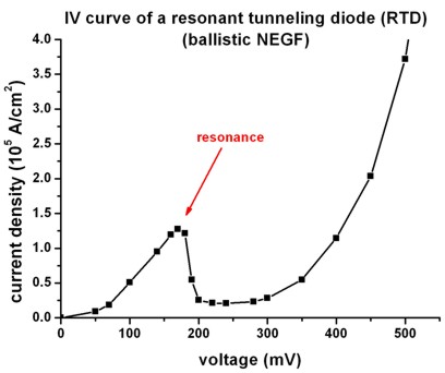
The following figure shows the IV characteristics of the resonant tunneling diode.
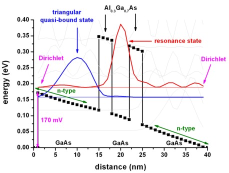
Schrödinger equation with Dirichlet boundary conditions at 0 nm and 40 nm The following figure shows the self-consistently calculated conduction band
profile of the GaAs/AlGaAs resonant tunneling structure plotted at the resonant
bias voltage of 170 mV including the wave functions (psi2). Note that
these wave functions do not necessarily correspond to reality as we imposed
artificially high (i.e. infinite) barriers to the left and right side of the
sample region by applying Dirichlet boundary conditions to the Schrödinger
equation (i.e. psi = 0 at 0 nm and at 40 nm). We also note that these
wave functions are not used in the NEGF formalism. They are only shown for a
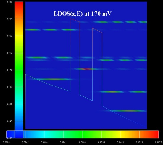
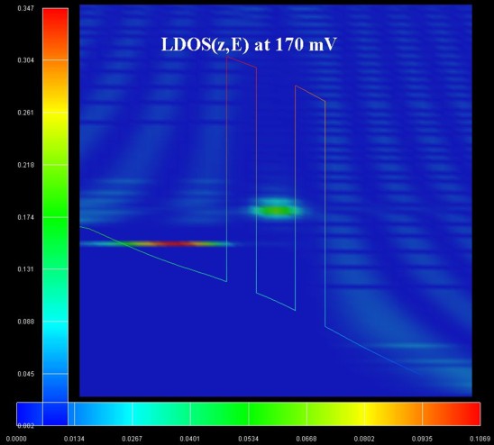
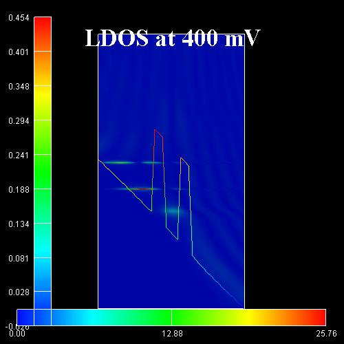
qualitative understanding of the structure. The right figure shows the local density of states LDOS(z,E) of the simulated
structure. Note that the Schrödinger equation for this structure was simulated
with Dirichlet boundary conditions (psi = 0) at z = 0 nm and z = 40 nm. This
will lead to artificially confined states that are not present in a simulation
where "open boundaries" are used.
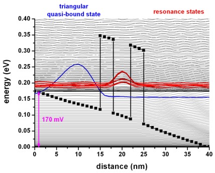
Schrödinger equation with Dirichlet boundary conditions at -300 nm and 340 nm A more realistic picture of the wave functions can be obtained by calculating
the wave functions for the same structure but this time including a flat-band
region of 300 nm region to the left and to the right of the structure mimicking
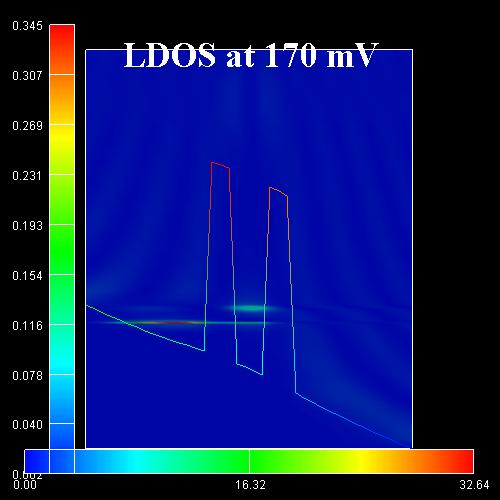
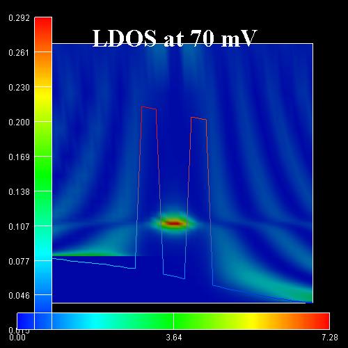
some kind of "open boundaries". The right figure shows the local density of states LDOS(z,E) of the simulated
structure. Note that the Schrödinger equation for this structure was simulated
with Dirichlet boundary conditions (psi = 0) at z =
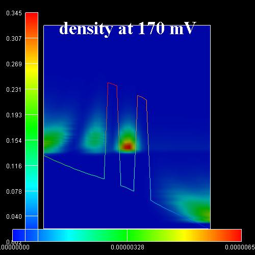
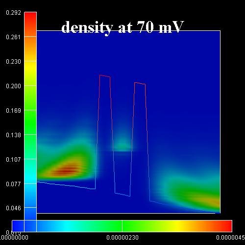
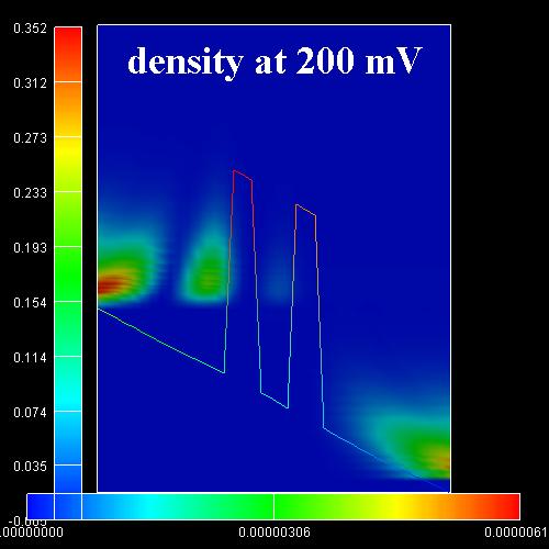
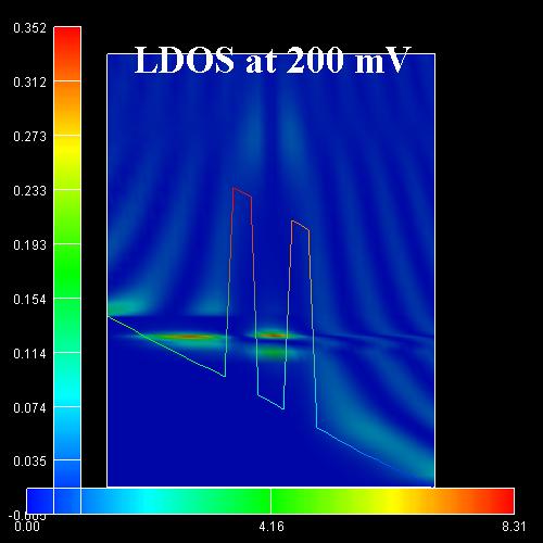
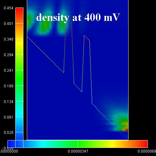
Results of ballistic NEGF calculationsEnergy resolved electron density and energy resolved local density of states (LDOS)The following figure shows the self-consistently calculated conduction band
profile of the GaAs/AlGaAs resonant tunneling structure plotted at the resonant
bias voltage of 170 mV together with Including scatteringT. Kubis and P. Vogl showed in their above cited paper, that due to scattering, the triangular quasi-bound state will be filled by electrons that have a "high" energy at the left contact, and then lose energy by scattering events and thus fill this triangular bound-state. The peak current in the I-V characteristic then occurs at a bias voltage where this quasi-bound state is aligned with the resonant quantum well state. Assuming ballistic transport, the electrons in the contact fly towards the barrier, maintaining their (high) energy and therefore hit the resonance energy in the well at a significantly lower bias as compared to a calculation including scattering where the electrons lose energy to occupy the triangular quasi-bound state. In the ballistic case, the I-V characteristic is then entirely determined by the properties of the contact rather than by the doping of the device. A careful inclusion of all inelastic processes is therefore necessary to capture the physical mechanisms that determine the resonance bias and peak (and valley) value of the RTD. For the results of the calculations including scattering (and a discussion of it), we refer to the section 4 of the above mentioned paper:
|
|
|