nextnano3 - Tutorial
1D Tutorial
Schrödinger-Poisson - A comparison to the tutorial file of Greg Snider's
code
Author:
Stefan Birner
==> This is the old website:
A new version of this tutorial can be found
here.
-> Greg_Snider_MANUAL_1D_nn3.in
/ *_nnp.in -
input file for nextnano³
and nextnano++ software
-> Greg_Snider_MANUAL_1D_nn3_analytic.in / *_nnp.in -
-> Greg_Snider_MANUAL_2D_nn3.in
/ *_nnp.in -
-> Greg_Snider_MANUAL_2D_nn3_analytic.in
/ *_nnp.in -
input file for nextnano³
and nextnano++ software (analytic doping function)
We appreciate that Greg Snider (University of Notre Dame) provided his code,
the manual and the input files free of charge, so that we could use it here as a
test case.
His 1D Poisson/Schrödinger code can be obtained from here:
http://www.nd.edu/~gsnider/
This tutorial is based on his manual ('1D Poisson Manual.pdf',
MANUAL.EX).
Schrödinger-Poisson - A comparison to the tutorial file of Greg Snider's
code
We simulate a structure consisting of
| |
|
surface |
Schottky barrier of 0.6 V |
| |
15 nm |
GaAs |
n type doped (1018 cm-3) |
| |
20 nm |
Al0.3Ga0.7As |
n type doped (1018 cm-3) |
| |
5 nm |
Al0.3Ga0.7As |
|
| |
15 nm |
GaAs |
quantum well |
| |
50 nm |
Al0.3Ga0.7As |
|
| |
250 nm |
Al0.3Ga0.7As |
p type doped (1017 cm-3) |
| |
|
substrate |
|
The grid resolution is 1 nm with the exception of the 250 nm layer which has
a resolution of 5 nm.
The dopants are assumed to be fully ionized.
The temperature is 300 K.
The Schrödinger equation will be solved between 5 nm and 195 nm.
Doping profile
We consider two further impurity profiles resulting from ion implantation
using LSS theory.
The donor and
acceptor profiles are written out to the file "doping_concentration1D.dat"
and look as follows:
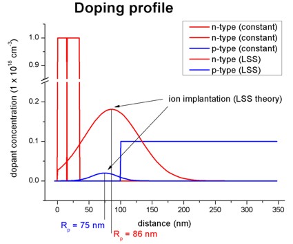
The relevant parameters are:
| |
implant |
dose [1/cm2] |
projected range Rp [nm] |
projected straggle Delta Rp [nm] |
| |
donor |
2 * 1012 |
86 |
44 |
| |
acceptor |
1 * 1011 |
75 |
20 |
For further details on the LSS theory (ion implantation) and on the doping
profiles, please check the relevant keyword
$doping-function.
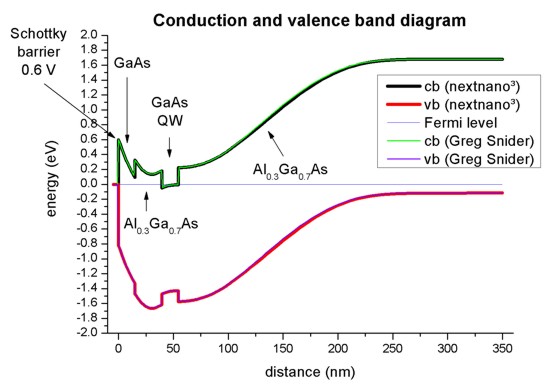
Conduction and valence band edges
The following figure shows the conduction and valence band edges as well as
the Fermi level (which is constant and has the value of 0 eV) for the structure
specified above. These bands are the solutions of the the self-consistent
Schrödinger-Poisson equation.
Both codes, nextnano³ and Greg Snider's "1D Poisson" lead to the same
results.
Electron eigenstates and eigenfunctions
Inside the GaAs quantum well there are three confined electron states. The
ground state is below the Fermi level and thus occupied.
The following figure shows a zoom of the GaAs Quantum well.
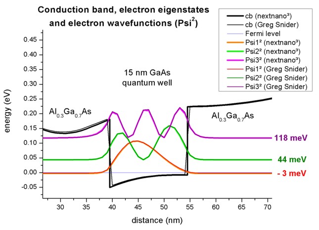
The wave functions as calculated with nextnano³ are nearly identical to
Greg Snider's "1D Poisson" code, as well as the energies.
However, there are tiny differences which is not too suprising as the conduction
band profile is not completely identical:
nextnano³ uses
multiple points at material interfaces which lead to sharp (abrupt)
interfaces.
nextnano³ interface: 39.5 nm (two grid points, one for GaAs and one for
AlGaAs)
54.5 nm (two grid points, one for GaAs and one for AlGaAs)
Greg Snider's interfaces: There is a grid point at 39 nm (AlGaAs) and the next
one at 40 nm (GaAs),
and at 54 (GaAs) nm and the next one at 55 nm (AlGaAs).
Thus at 39.5 and 54.5 nm, an interpolated value is used in the plot of the
conduction band diagram.
| Electron states |
nextnano³ |
Greg Snider's "1D Poisson" code |
| E1 [meV] |
- 3.0 |
- 1.3 |
| E2 [meV] |
43.5 |
44.0 |
| E3 [mV] |
117.5 |
117.8 |
Electron and hole densities
The electron and hole densities are depicted in this figure. Again, there is
also nice agreement between the two codes.
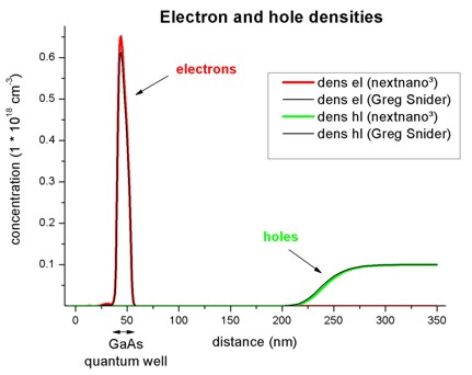
The integrated electron density in the
GaAs quantum well region is 0.664 * 1012
cm-2. (Greg Snider's result: 0.636 * 1012
cm-2)
The integrated hole density in the right
most Al0.3Ga0.7As region is 1.033
* 1012 cm-2. (Greg Snider's result: 1.085
* 1012 cm-2)
The relevant output files are:
- densities/int_el_dens.dat

- densities/int_hl_dens.dat
This tutorial shows very nicely that both codes, nextnano³ and Greg
Snider's "1D Poisson" lead to the same results.
Greg Snider's 1D Poisson/Schrödinger code can be obtained from here:
http://www.nd.edu/~gsnider/
2D simulations
-> Greg_Snider_MANUAL_2D_nn3.in / *_nnp.in
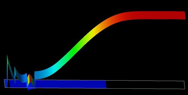
The following figure shows the conduction band profile and the ground state
wave function (probability density psi²) of the same structure in a 2D simulation
where the y direction has been assumed to be of length 100 nm with periodic
boundary conditions.
|