nextnano3 - Tutorial
next generation 3D nano device simulator
1D Tutorial
Electron density of states (DOS) of a GaAs quantum well with infinite barriers
and
hole density of states (DOS) of a Si hole channel (triangular potential)
Author:
Stefan Birner
If you want to obtain the input files that are used within this tutorial, please
check if you can find them in the installation directory.
If you cannot find them, please submit a
Support Ticket.
-> 1D_DOS_GaAsQW_10nm.in

-> 1D_DOS_GaAsQW_20nm.in

-> 1D_DOS_GaAsQW_100nm.in

-> 1DSi_triangular_DOS_holes.in
1) Electron density of states (DOS) of a GaAs quantum well with infinite barriers
-> 1D_DOS_GaAsQW_10nm.in

-> 1D_DOS_GaAsQW_20nm.in

-> 1D_DOS_GaAsQW_100nm.in
Here, we calculate the density of states (DOS) for the electrons in a 10 nm, 20 nm
and 100 nm
GaAs quantum well using infinite barriers.
We are using the 8-band k.p model and calculate the energy dispersion E(k||)
= E(kx,ky).
However, for simplicity, and in order to be able to check our k.p results
with analytical results of the single-band approximation (i.e. parabolic and
isotropic energy dispersion), we modify our 8-band k.p parameters so that the coupling
between electrons and holes is switched off. Consequently, we are using an
isotropic and parabolic effective mass of 0.067 [m0] for our 8-band
k.p model.
The density of states for a single subband in a (GaAs) quantum well system can be calculated
to be:
rho2D(E) = m*
/ (pi hbar2) =
= 0.067
[m0] / (pi hbar2) =
= 0.067
* 2.607275116 * 1037 J-1 m-2 =
= 0.067
* 4.177314998 * 1018 eV-1 m-2 =
=
1.746874328 * 1036 J-1 m-2 =
=
2.798801048 * 1017 eV-1 m-2
[m0] / (pi hbar2) = 2.607275116 * 1037 J-1 m-2
= 4.177314998 * 1018 eV-1 m-2
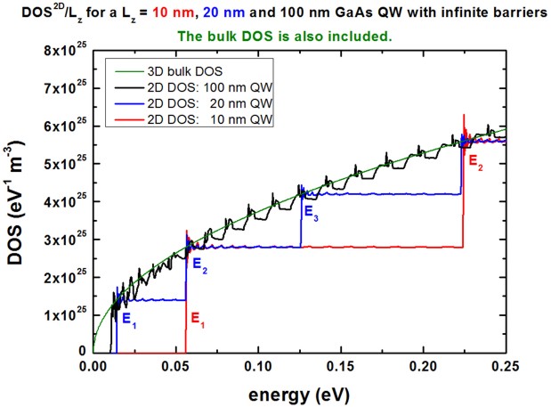
The following figure shows the electron density of states (DOS) as a function
of energy for a GaAs QW with infinite barriers.
The QW width has been assumed to be Lz = 10 nm, Lz = 20 nm
and Lz = 100 nm.
In order to compare the four cases
- 10 nm QW
- 20 nm QW
- 100 nm QW
- bulk (analytical formula)
we scale
rho2D(E) by dividing by the length of the QW:
rho2D ' (E) =
rho2D(E) / Lz
where Lz is the length of the QW. Then rho2D ' in units of eV-1 m-3.

For a QW, a sharp steplike density of states is obtained, in contrast to the
bulk case where a E1/2 dependence is expected.
(The bulk curve has been calculated analytically.)
Our results are in excellent agreement with analytical results for the
two-dimensional DOS (e.g. compare with P. Harrison, Quantum wells, wires and
dots or S.L. Chuang, Physics of optoelectronic devices).
The DOS output is contained in the following file: DOS_el_sum_norm.dat
The first column contains the energy in units of [eV], the second column the DOS
(sum over all subbands) in units of [eV-1 m-2].
The DOS output for each individual subband is contained in this file: DOS_el_norm.dat
The first column contains the energy in units of [eV], the other columns
the DOS of each individual subband in units of [eV-1 m-2].
Note: The nextnano³ output DOS_el_sum.dat depends on the size of the k||
space region: ~ 1 / k||,max2
For this output, it seems
that the spin is included twice. So these values have to be divided by "2".
The nextnano³ output
DOS_el_sum_norm.dat does not depend on the size of the k||
space region. The spin factor is correct.
The following parameters were used:
- 10 nm QW: 0.25 nm grid resolution; 3000 k||
points in total, i.e. 351 k||
have to be calculated
- 20 nm QW: 0.50 nm grid resolution; 3000 k||
points in total, i.e. 351 k||
have to be calculated
- 100 nm QW: 1.00 nm grid resolution; 3000 k||
points in total, i.e. 351 k||
have to be calculated
The following interesting question arises:
- How does the DOS look like for a QW with finite barriers and
an anisotropic and nonparabolic effective mass tensor (8-band k.p)?
Comment: There are different definitions of the density of states.
- P. Harrison: rho2D(E) = m*
/ (pi hbar2)
- G.
Bastard: rho2D(E) = m*
/ (pi hbar2) * Lx Ly
- S.L.
Chuang: rho2D(E) = m*
/ (pi hbar2) / Lz
Other results (benchmark):
- Paul Harrison for a 20 nm GaAs QW with infinite barriers:
1.746847 * 1036 J-1 m-2 =
2.798757 * 1017 eV-1 m-2 for an electron
mass of m* = 0.067 [m0].
This corresponds to
rho2D ' (E) =
rho2D(E) / Lz = 1.399 * 1025 eV-1 m-3
f
- S.L. Chuang for a 10 nm GaAs QW (p. 90) at the first step (E1
= 56.5 meV): 2.78 * 1025 eV-1 m-3
- S.L. Chuang for bulk GaAs (p. 90): 100 meV above Ec: 3.69 * 1025 eV-1 m-3
2) Hole density of states (DOS) of a Si hole channel (triangular potential)
-> 1DSi_triangular_DOS_holes.in
Here, we calculate the density of states (DOS) for the holes in a 10 nm wide
Si channel that is modeled by a triangular potential, corresponding to an
applied electric field of 5 MV/cm.
- A 1 nm SiO2 oxide layer is included in the simulations.
- The Si/SiO2 valence band offset (VBO) was assumed to be 4.3
eV.
- The grid spacing in real space was 0.1 nm.
- The following 6-band k.p parameters are employed for both the Si and
the SiO2 layer:
  6x6kp-parameters = -6.53d0  -4.64d0
	-8.32d0 ! L, M, N


	0.044d0
! Deltasplit-off [eV]
Note that our L, M, N parameters are the same as in
M.V. Fischetti, JAP 80, 2234 (1996)
but Fischetti's parameters (L',M',N) have to be converted
because his parameters are defined differently.
==> L = L' - 1, M = M' - 1, N = N'
- The energy dispersion E(kx,ky) is discretized on a
square up to kx,max = ky,max = 0.7 [1/Angstrom]
 k-range         =
	0.7d0 ! [1/Angstrom]
 num-kp-parallel = 4761  ! 4761
	= 595 x 8 + 1
using a total of 4761
points in the two-dimensional (kx,ky) space.
Due to symmetry, we only have to discretize ~1/8th of the total 2D
k|| space, i.e. the 6-band k.p Hamiltonian (dimension
of matrix: 600 x 600) has to be diagonalized 595 times.
This tutorial is similar to the following paper:
Hole transport in p-channel Si MOSFETs
S. Krishnan, D. Vasileska, M.V. Fischetti
Microelectronics Journal 36, 323 (2005)
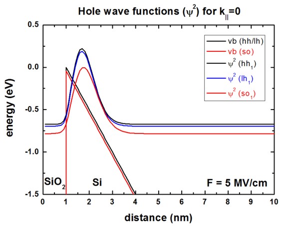
The following figure shows the valence band edges of heavy,
light and split-off
hole at an electric field of 5 MV/cm.
The heavy and light hole valence band edges are degenerate because the silicon
layer is assumed to be unstrained.
The square of the wave functions of the heavy hole,
light hole and split-off hole
are also shown.
At k|| = 0, the energies and the squares of the spin-up and
spin-down wave functions are identical.
This is not the case for k|| /= 0 because the quantum well
potential is unsymmetric.

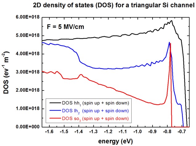
The following figure shows the two-dimensional density of states (DOS) for
the holes in the 10 nm triangular Si channel at an electric field of 5 MV/cm.
At k|| /= 0 the energies for spin-up and spin-down states are
not equal any more leading to different DOS for spin-up and spin-down.
Here, we want to emphasize the different DOS for heavy hole,
light hole and
split-off hole (thus we added the spin-up and spin-down DOS for each
subband).
One can nicely see that the hole DOS differs dramatically from the step-like DOS
of the analytical isotropic and parabolic effective-mass approximation. Only the
heavy hole DOS is close to this simple approximation.

With respect to this energy scale, the valence band maximum is located at 0 eV.
At k|| = 0,
- the top-most heavy hole state is at Ehh1
= -0.672 eV
- the top-most light
hole state is at Elh1 = -0.696 eV
- the top-most split-off hole state
is at Eso1 = -0.784 eV.
Our heavy and light hole DOS is in good agreement with the paper of Krishnan
et al. However, the split-off hole DOS differs.
Namely, it is not clear why Krishnan's split-off hole DOS seems to start at an
energy which is equal to the heavy hole energy.
See also this tutorial for more information on the energy dispersion E(kx,ky)
of a triangular Si channel:
k|| energy dispersion
of holes in unstrained and strained silicon inversion layers
|