| nextnano.com nextnano³ Download | Search | Copyright | Publications * password protected |
nextnano³ software
|
|
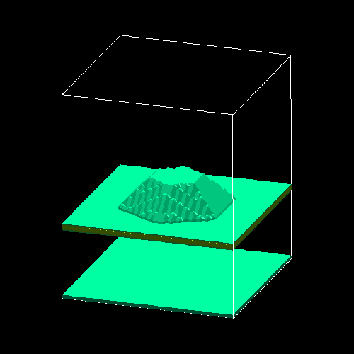
| 3D hexagonal GaN QD (wurtzite) |
|
|
|
|
|
nextnano3 - Tutorialnext generation 3D nano device simulator3D TutorialHexagonal shaped GaN quantum dot embedded in AlN (wurtzite)Author: Stefan Birner If you want to obtain the input files that are used within this tutorial, please
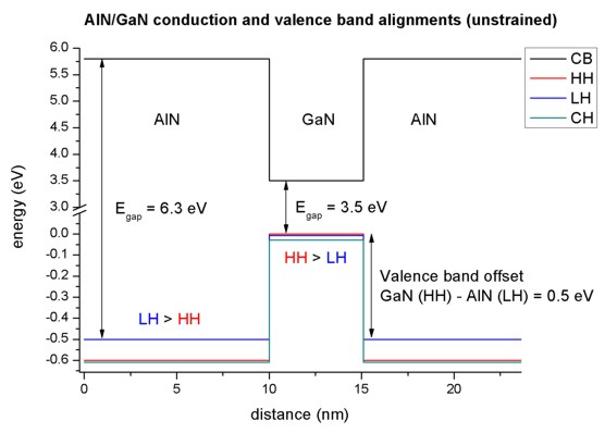
check if you can find them in the installation directory. Introduction: Conduction and valence band alignment in AlN/GaN (unstrained)
The following figure shows the conduction and valence band edge alignment in AlN/GaN structures (unstrained). In AlN, the light hole (LH) is the highest valence band whereas in GaN, this is the heavy hole (HH). We assumed a valence band offset of VBO = 0.5 eV, the conduction band offset is much larger (CBO = 2.3 eV). All material parameters are based on the paper
although meanwhile better parameters are available.
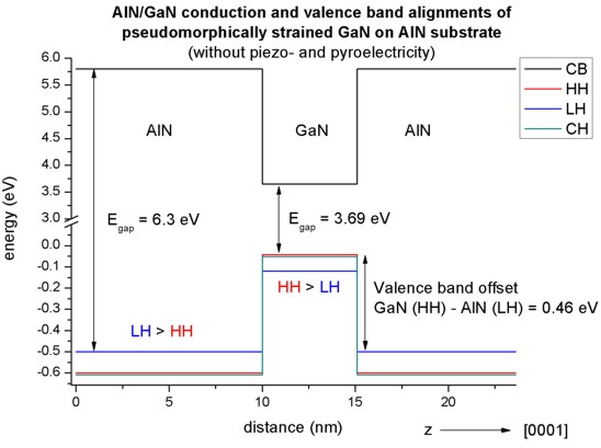
Conduction and valence band alignment in AlN/GaN of pseudomorphically strained GaN on AlN substrate
The lattice constants of GaN are larger than in AlN, thus GaN is
compressively strained.
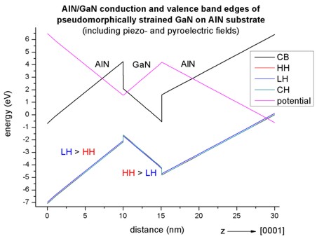
Conduction and valence band edges in AlN/GaN of pseudomorphically strained GaN on AlN substrate including piezo- and pyroelectric fields
This figure also includes the electrostatic potential which is the solution of the Poisson equation taking into account the piezo- any pyroelectric interface (and surface) charges. The piezo- and pyroelectric fields tilt the band edges
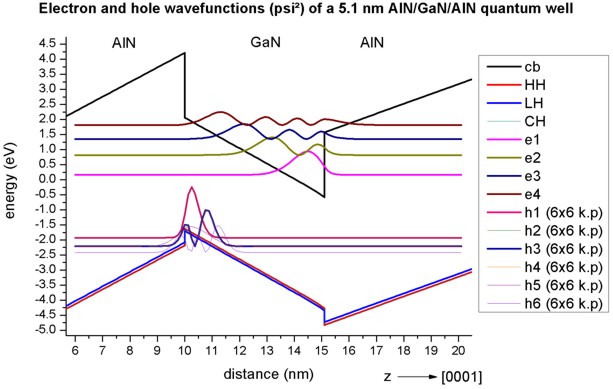
Electron and hole wave functions in an AlN/GaN/AlN quantum well
The following figure shows the electron and hole wave functions (psi²) in a 5.1 nm AlN/GaN/AlN quantum well. For the electrons, the single-band effective-mass approximation was used whereas for the holes the 6-band k.p model was used. The figure shown the four lowest electron eigenstates and the 6 highest valence band eigenstates. All eigenstates are two-fold degenerate due to spin.
Hexagonal shaped GaN quantum dot embedded in AlN (wurtzite)This tutorial is based on the following paper:
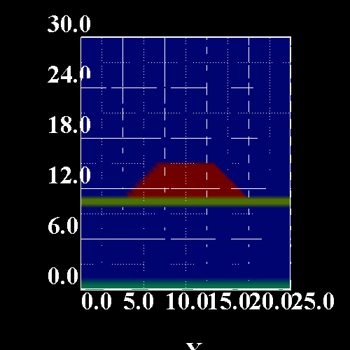
The simulated hexagonal GaN quantum dot (height = 4 nm) is embedded in an AlN matrix. The wetting layer is 1 nm thick and consists of GaN.
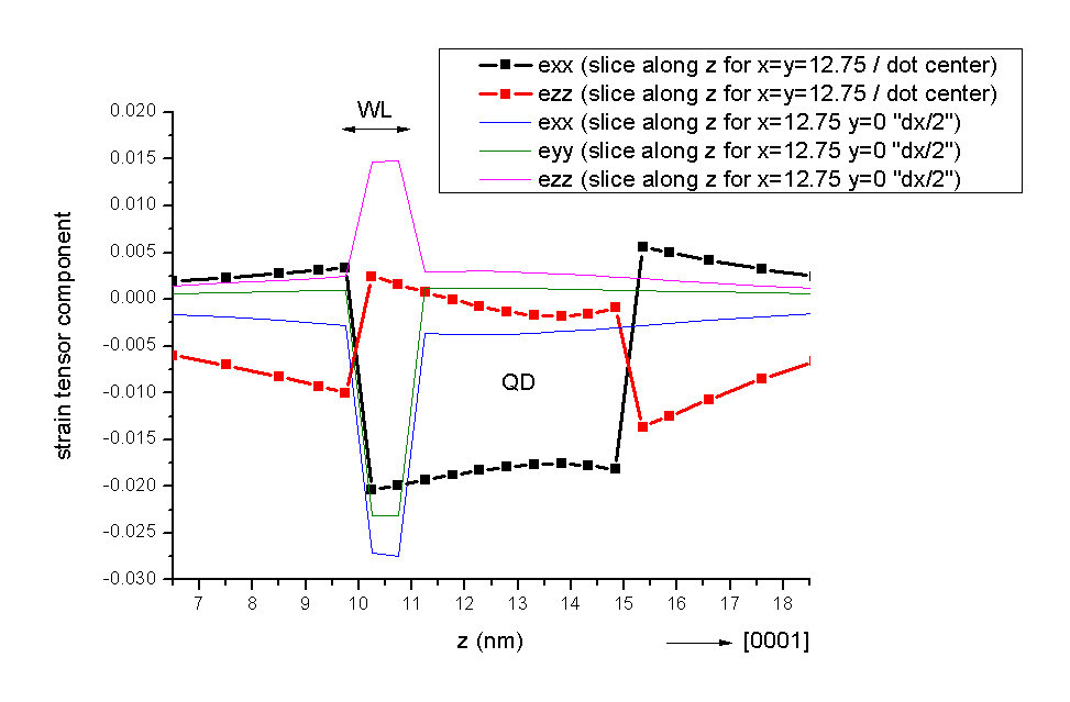
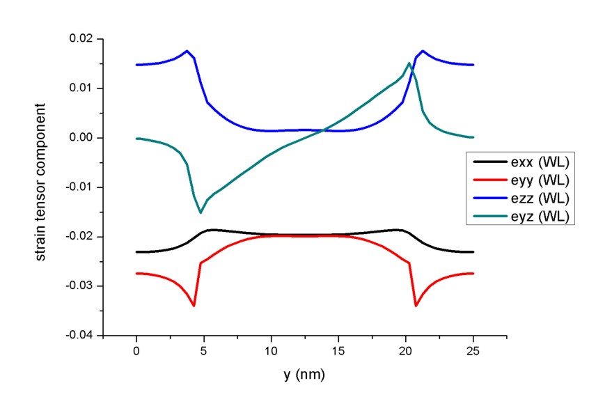
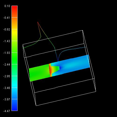
The strain tensor components of a line through the center of the quantum dot
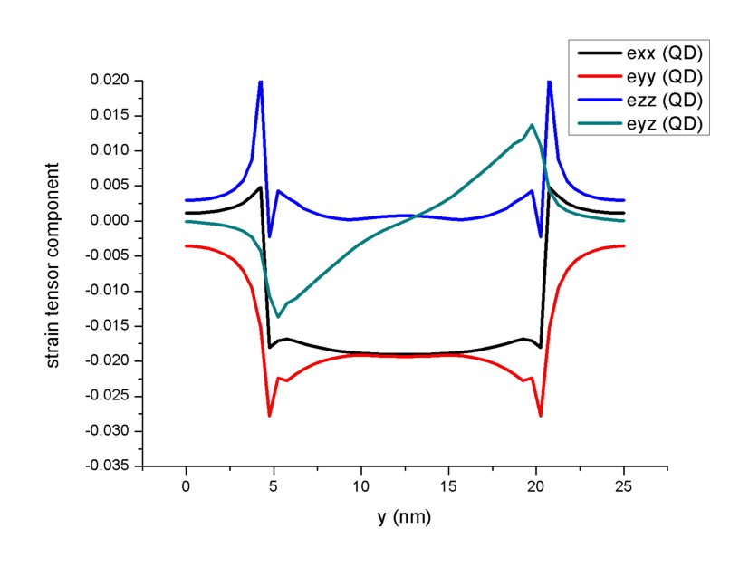
along the z axis are shown here. The following figures show the strain tensor components along the [10-10]
direction (x direction) for a line through the bottom of the quantum dot and for
a line through the wetting layer.
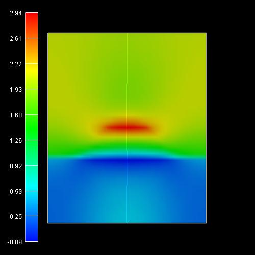
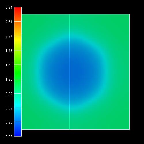
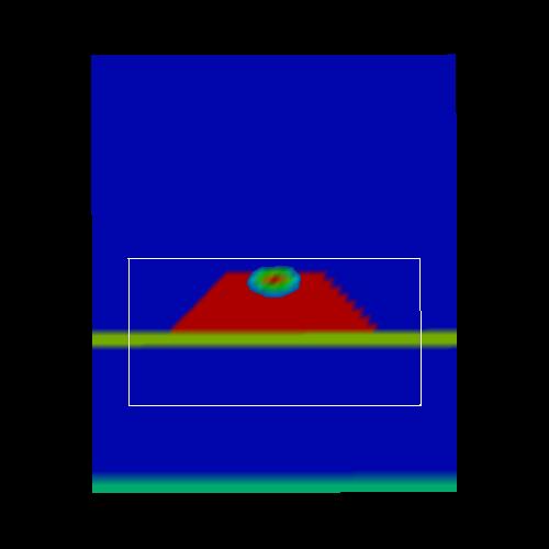
The conduction (left) and valence band edges (right) are shown in the
following figures.
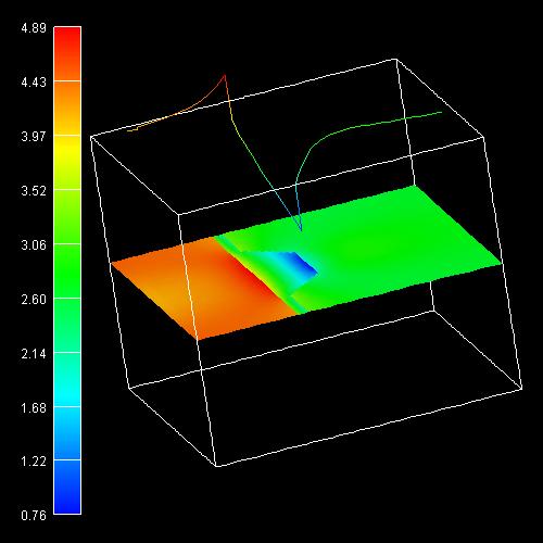
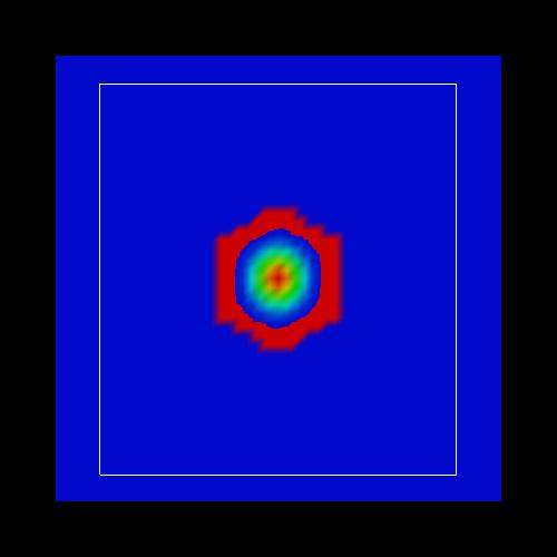
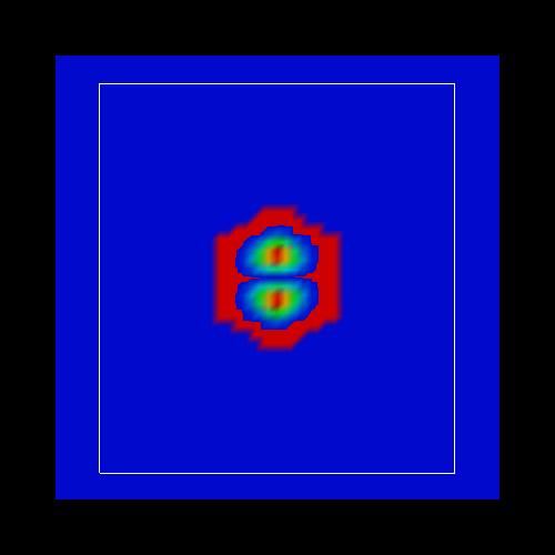
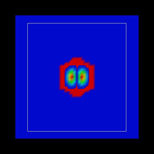
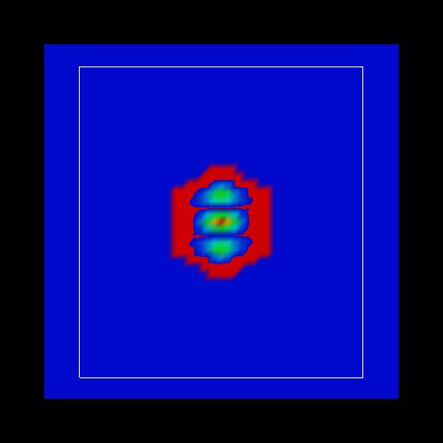
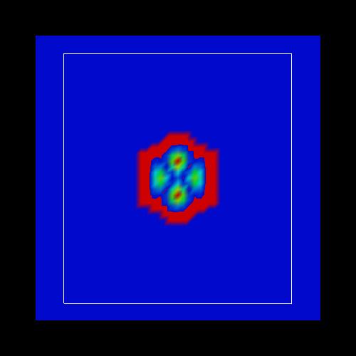
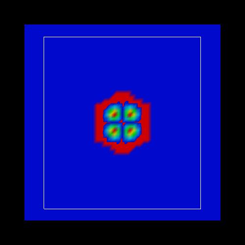
The electron states are located near the top of the quantum dot where the
conduction band has a minimum. The following figures show the six lowest electron states of the quantum dot. The 2nd and 3rd eigenstates are degenerate, as well as the 4th, 5th and 6th.
The figures of the wave functions (psi²) are related to Fig. 7 in the cited paper of Andreev/O'Reilly. |
|
|