Simple quantum cascade structure
- Input Files:
1DQCL_simple_nnp.in
In this tutorial we simulate a simple quantum cascade structure that has been presented in an article by Capasso et al. (Figures 12 (b) and 16 (b) of [CapassoIEEE1986]).
We can generate the following picture that is based on Fig. 3 of [BirnerPhotonikInt2008] and [BirnerPhotonik2008].
It shows the conduction band edge profile of an Al0.48In0.52As/In0.53Ga0.47As superlattice at an electric field of -89 kV/cm.
The single-band effective-mass Schrödinger equation is solved for this band profile.
The wave functions (
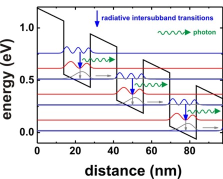
The basic idea of such a structure is to depopulate the lowest eigenstate of each quantum well efficiently by bringing it into resonance with the third eigenstate of the next quantum well (resonant tunneling).
The transition second eigenstate
On the other hand, the transition third eigenstate
Another important condition for a quantum cascade laser is population inversion, i.e. the occupation of the third eigenstate must be much higher than the occupation of the second eigenstate and lowest eigenstate.
The input file 1DQCL_simple_nnp/*nn3.in should be rather intuitive and self-explanatory. Documentation for each keyword and each specifier can be found here: Keywords
In the nextnano++ sample file, the electric field is applied by specifying the keyword
contactsas follows:contacts{ charge_neutral{ name = "leftgate" bias = 0.0 } charge_neutral{ name = "rightgate" bias = 1.36081 # corresponds to electric field of F = -89 kV/cm } }
In the keyword
structure, “leftgate” is defined atx = [-1, 0]and “rightgate” is atx = [152.9, 153.9]. Thus the electric field applied by this specification is -1.36081 [V] / 152.9 [nm] = -89 [kV/cm]Alternatively, we can apply a constant electric field by providing a value for the field.
poisson{
   electric_field{ strength = -89e5 } # [V/m]
   output_potential{}
   output_electric_field{}
}
Output
The output files are ASCII files.
Bandedges
The conduction and valence band edges can be found in the following file:
bias_0000/Quantum/bandedges.dat (nextnano++)
band_profile/cb_Gamma.dat (nextnano³, conduction band edge only)
If one plots the conduction band profile, one gets the following figure.
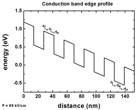
There are six Al0.48In0.52As barriers and five In0.53Ga0.47As wells. The conduction band offset is 0.51 eV.
Eigenvalues
The 40 eigenvalues that were calculated can be found in these files. The units are [eV].
bias_0000/Quantum/wf_energy_spectrum_quantum_region_Gamma_0000.dat (nextnano++)
wavefunctions/ev_cb1_sg1_deg1.dat (nextnano³)
The eigenvalues are also contained in these files, i.e. the eigenvalues for each grid point
bias_0000/Quantum/wf_probabilities_shift_quantum_region_Gamma_0000.dat (nextnano++)
wavefunctions/cb1_sg1_deg1_psi_squared_shift.dat (nextnano³)
1st column |
2nd column |
3rd column |
… |
41st column |
grid points in units of [nm] |
1st eigenvalue in units of [eV] |
2nd eigenvalue in units of [eV] |
… |
40th eigenvalue in units of [eV] |
If one plots these columns (together with the conduction band edge) one obtains the following picture:
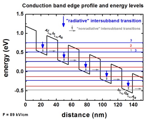
Note
The figure shows only the following energy levels: 1,2,3,4,5,9,10,12,16,18,20,26,27,30,37
Wave Functions
The square of the wave functions (
bias_0000/Quantum/wf_probabilities_shift_quantum_region_Gamma_0000.dat (nextnano++)
wavefunctions/cb1_qc1_sg1_deg1_psi_squared_shift.dat (nextnano³)
1st column |
… |
42nd column |
43rd column |
… |
81st column |
grid points in units of [nm] |
… |
… |
Note
In order to be able to plot the wave functions nicely into the conduction band edge profile, we shift the square of the wave function by its corresponding energy.
If one plots these columns (together with the conduction band edge) one obtains the following picture:
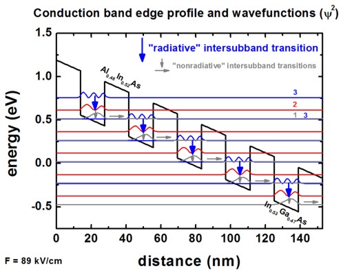
Note
The figure shows only the following wave functions: 1,2,3,4,5,9,10,12,16,18,20,26,27,30,37
Now the lowest eigenstate of each quantum well is in resonance with the third eigenstate of the next quantum well. This leads to the depopulation of the lowest eigenstate of each quantum well.
Photon should be emitted with the radiative intersubband transition 3
Effective masses
The effective masses that were used for each grid point can be found in these files.
Structure/charge_carrier_masses.dat (nextnano++)
material_parameters/conduction_band_masses.dat (nextnano³)
Note
We need to add the following option into the sample file for nextnano++.
output{
    material_parameters{
        charge_carrier_masses{ boxes = yes }
        }
    }
1st column: grid points in units of [nm]
other columns:
nextnano++: effective mass tensor components of Gamma and HH valley in units of [m0]. When we use other valleys for the simulation, then these columns shows the effective mass tensor components in that valleys.
nextnano³: effective mass tensor components of Gamma, L and X valleys in units of [m0].
These masses have been calculated from the binaries InAs, GaAs and AlAs for the relevant ternaries, including bowing parameters.
Intersubband matrix elements
Experienced users might be interested in having a look at the intersubband matrix elements.
We can find the intersubband (or intraband) matrix elements quantum{ } in 1DQCL_simple_nnp.in:
intraband_matrix_elemets{
    Gamma{}
    output_matrix_elements = yes
    output_transition_energies = yes
    output_oscillator_strengths = yes
}
The relevant output files are
bias_0000/Quantum/intraband_matrix_elements_quantum_region_Gamma_100.txt (nextnano++)
bias_0000/Quantum/transition_energies_quantum_region_Gamma_Gamma.txt (nextnano++)
In the output file of the nextnano³ sample file, we can already have them here:
wavefunctions/intraband_pz_cb1_sg1_deg1.txt (nextnano³)
See Optical spectra for more information on the matrix elements.
- Input Files for nextnano³:
1DQCL_simple_nn3.in
Last update: 28/05/2024