— SOON — Hexagonal shaped GaN quantum dot embedded in AlN (wurtzite)
Attention
Figures in this tutorial are transferred from old documentation and are consistent with nextnano³ input files. They differ from results obtained with nextnano++ as these input file has been improved, including change of simulation domain and boundary conditions, to represent results from the cited publication more accurately. However, qualitative tendencies are preserved.
Header
- Input files in examples\quantum_dots\:
QD_GaN_Andreev_PRB_2000_1D_nnp_band-offsets.in
QD_GaN_Andreev_PRB_2000_1D_nnp_strain.in
QD_GaN_Andreev_PRB_2000_1D_nnp_strain-PzPr-poisson-1b.in
QD_GaN_Andreev_PRB_2000_1D_nnp_strain-PzPr-poisson-6kp.in
QD_GaN_Andreev_PRB_2000_3D_nnp.in
- Scope:
In this tutorial we investigate the influence of strain and pyro-/ piezoelectric fields on the electronic structure of hexagonal shaped GaN/ AlN quantum dots. The tutorial is based on [Andreev2000].
Conduction and valence band alignment in AlN/GaN QWs (unstrained)
In this section the input file QD_GaN_Andreev_PRB_2000_1D_nnp_band-offsets.in is used to compute band offsets.
Figure 2.4.8.27 shows the conduction and valence band edge alignment in AlN/GaN structures (unstrained). In AlN, the light hole (LH) is the highest valence band whereas in GaN, this is the heavy hole (HH). We assumed a valence band offset of VBO = 0.5 eV, the conduction band offset is much larger (CBO = 2.3 eV). All material parameters are based on [Andreev2000] although meanwhile better parameters are available.
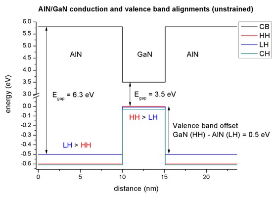
Figure 2.4.8.27 Conduction band edge (CB) and valance band edges (HH, LH, CH) of the 1D AlN/ GaN QD (unstrained).
Conduction and valence band alignment in AlN/GaN QWs (pseudomorphically strained)
In this section the input file QD_GaN_Andreev_PRB_2000_1D_nnp_strain.in is used to show impact of the strain on the band edges without piezo effects.
Figure 2.4.8.28 shows the conduction and valence band edge alignment in the AlN/GaN structure, which is strained with respect to the AlN substrate. The lattice constants in GaN are larger than in AlN, thus GaN is compressively strained. The AlN band edges are the same as in Figure 2.4.8.27, only the GaN edges have changed:
The band gap of GaN has increased (compressive strain increases the band gap).
Now the crystal-field split-hole (CH) in GaN lies above the light hole (LH) and close to the heavy hole (HH).
The valence band offset has decreased to VBO = 0.46 eV.
The conduction band offset has decreased to CBO = 2.15 eV.
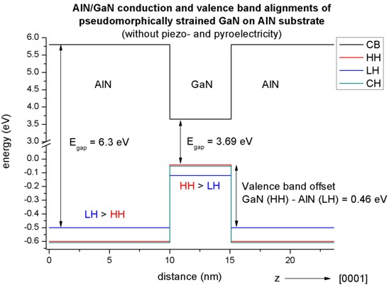
Figure 2.4.8.28 Conduction band edge (CB) and valance band edges (HH, LH, CH) of the 1D AlN/GaN QD (strained on AlN substrate).
Conduction and valence band edges in AlN/GaN QWs (pseudomorphically strained, including piezo- and pyroelectric fields)
In this section the input file QD_GaN_Andreev_PRB_2000_1D_nnp_strain-PzPr-poisson-1b.in or QD_GaN_Andreev_PRB_2000_1D_nnp_strain-PzPr-poisson-6kp.in can be used to observe piezo effect on the design.
In Figure 2.4.8.29 the effect of piezo- and pyroelectric fields on the band edge is shown. The band edge gets tilted due to the additional electric potential arising from the piezo- and pyroelectric charges. The electrostatic potential which is the solution to the Poisson equation is also shown in Figure 2.4.8.29.
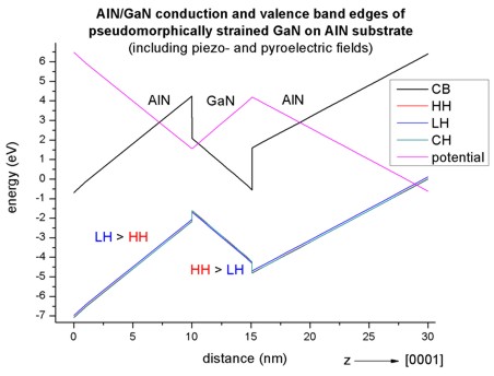
Figure 2.4.8.29 Conduction band edge (CB) and valance band edges (HH, LH, CH) of the 1D AlN/GaN QD (strained on AlN substrate) including piezo- and pyroelectric fields.
Electron and hole wave functions in AlN/GaN QWs
Figure 2.4.8.30 shows the electron and hole wavefunctions (\(\Psi^2\)) in a 5.1 nm AlN/GaN/AlN quantum well. For the electrons, the single-band effective-mass approximation was used whereas for the holes the 6-band k.p model was used. The figure shows the four lowest electron eigenstates and the 6 highest valence band eigenstates. All eigenstates are two-fold degenerate due to spin.
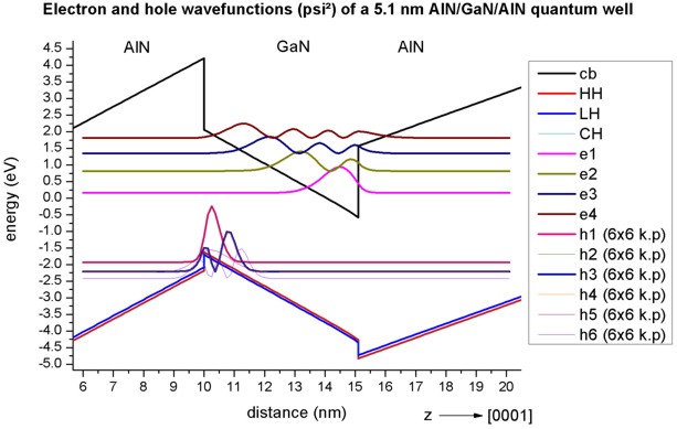
Figure 2.4.8.30 Electron and hole wavefunctions \(\Psi^2\) of a 5.1 mm AlN/GaN/AlN quantum well.
Hexagonal shaped GaN quantum dot embedded in AlN (wurtzite)
The simulated hexagonal GaN quantum dot (height = 4.1 nm) is embedded in an AlN matrix, input file QD_GaN_Andreev_PRB_2000_3D_nnp.in. The wetting layer is 1 nm thick and consists of GaN. The structure and a cross-section of the structure along x-y are shown in Figure 2.4.8.31 and Figure 2.4.8.32, respectively.
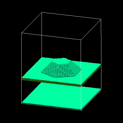
Figure 2.4.8.31 3D AlN/GaN quantum dot.
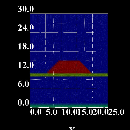
Figure 2.4.8.32 Cross-section of the hexagonal shaped AlN/GaN quantum dot.
The strain tensor components of a line through the center of the quantum dot along the z axis are shown in Figure 2.4.8.33. This figure is related to Fig. 2 (a) in [Andreev2000].
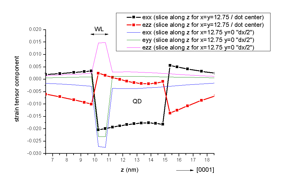
Figure 2.4.8.33 Strain tensor along the z-axis through the points (x, y) = (12.75, 12.75) nm and (x, y) = (12.75, 0) nm.
Figure 2.4.8.34 and Figure 2.4.8.35 show the strain tensor components along the [10-10] direction (y direction) for a line through the bottom of the quantum dot and for a line through the wetting layer, respectively. These figures are related to Fig. 2 (b) in [Andreev2000].
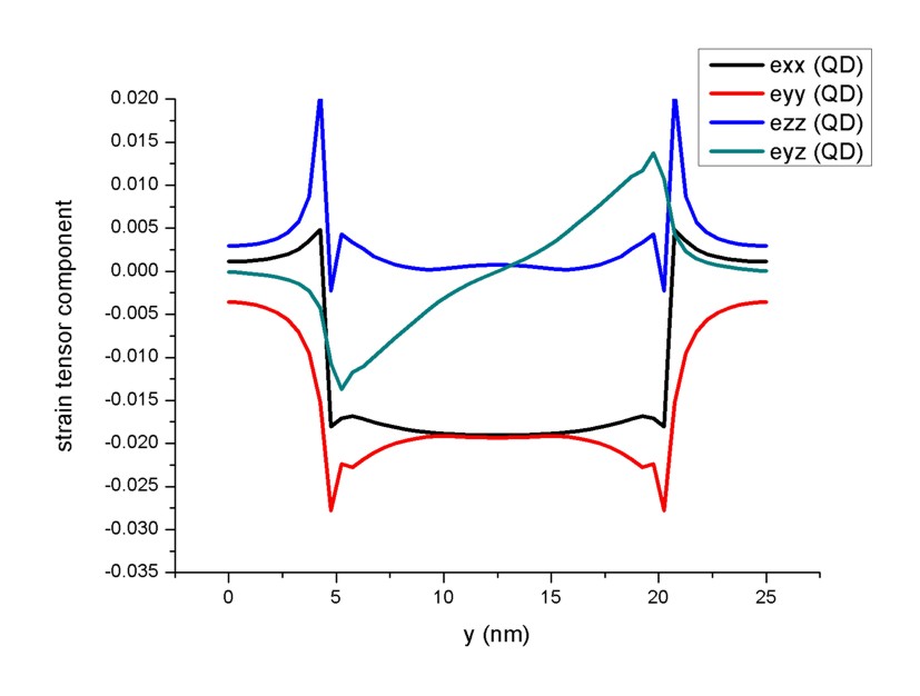
Figure 2.4.8.34 Strain tensor along the y-axis through the quantum dot (QD).
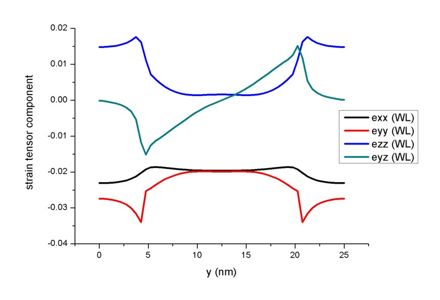
Figure 2.4.8.35 Strain tensor along the y-axis through the wetting layer (WL).
The strain induced piezoelectric fields and the pyroelectric fields lead to the electrostatic potential which is shown in Figure 2.4.8.36 and Figure 2.4.8.37. The figures of the potential are related to Fig. 4 in [Andreev2000]. In Figure 2.4.8.36 one can clearly see that the electrostatic potential has its maximum at the top of the QD and its minimum in the wetting layer area just below the QD. Figure 2.4.8.37 shows a cut of the electrostatic potential through the wetting layer plane.
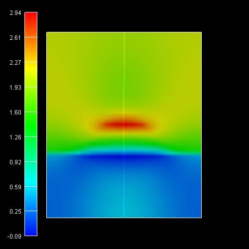
Figure 2.4.8.36 Electrostatic potential inside the quantum dot.
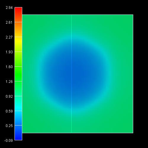
Figure 2.4.8.37 Electrostatic potential inside the wetting layer.
The conduction and valence band edges are shown in Figure 2.4.8.38 and Figure 2.4.8.39. One can clearly see that the conduction band minimum is located in the top of the quantum dot whereas the maximum for the valence band is located inside the wetting layer (WL) (which is equivalent to the bottom of the quantum dot). Thus, one expects the electrons, which are located in the top area of the QD, to be spatially separated from the holes, which are located in the WL (bottom of the QD). The energy scale is in units of [eV]. The figures of the conduction and valence band edges are related to Figs. 5 and 6 in [Andreev2000].
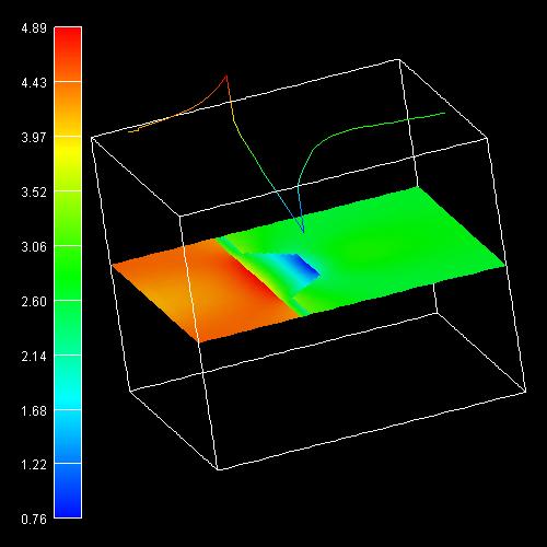
Figure 2.4.8.38 Conduction band edge of the QD.
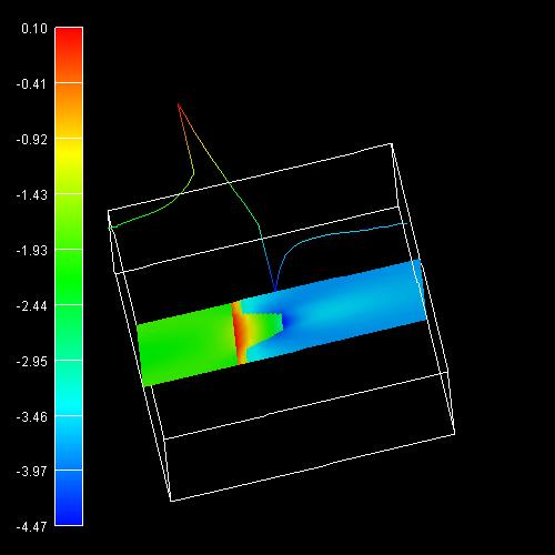
Figure 2.4.8.39 Valence band edge of the QD.
The electron states are located near the top of the quantum dot where the conduction band has a minimum. Figure 2.4.8.40 shows the electron ground state.
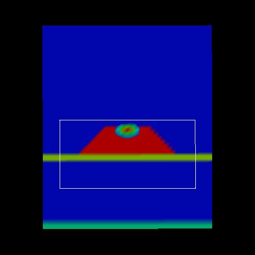
Figure 2.4.8.40 Electron ground state of the QD.
The following figures show the six lowest electron states of the quantum dot. The \(2^\mathrm{nd}\) and \(3^\mathrm{rd}\) eigenstates are degenerate, as well as the \(4^\mathrm{th}\), \(5^\mathrm{th}\) and \(6^\mathrm{th}\). The figures of the wave functions (\(\Psi^2\)) are related to Fig. 7 in [Andreev2000].
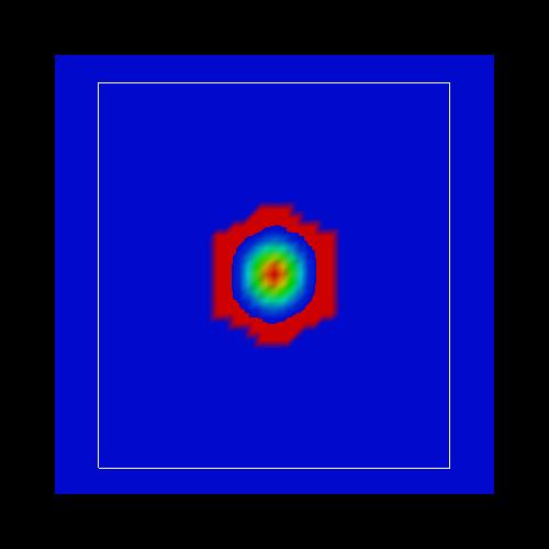
Figure 2.4.8.41 Probability density \(\Psi^2\) of the \(1^\mathrm{st}\) electron state in the QD.
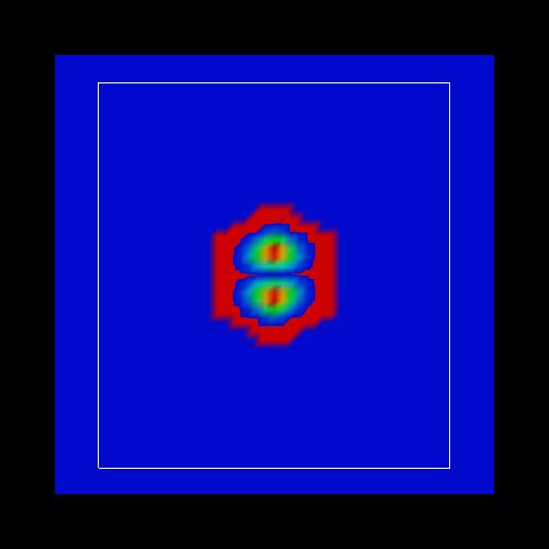
Figure 2.4.8.42 Probability density \(\Psi^2\) of the \(2^\mathrm{nd}\) electron state in the QD.
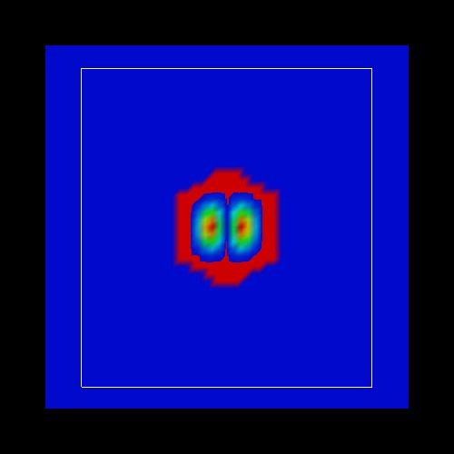
Figure 2.4.8.43 Probability density \(\Psi^2\) of the \(3^\mathrm{rd}\) electron state in the QD.
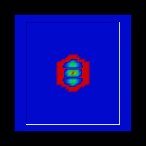
Figure 2.4.8.44 Probability density \(\Psi^2\) of the \(4^\mathrm{th}\) electron state in the QD.
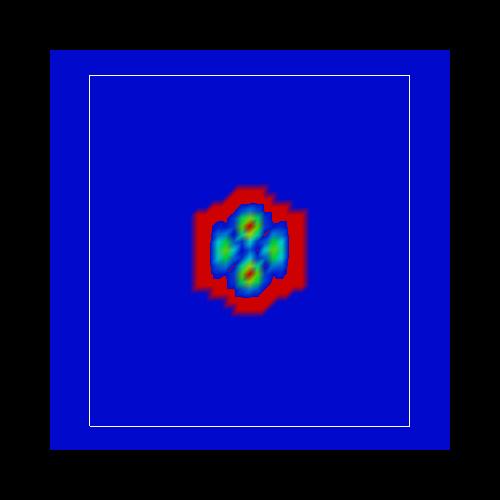
Figure 2.4.8.45 Probability density \(\Psi^2\) of the \(5^\mathrm{th}\) electron state in the QD.
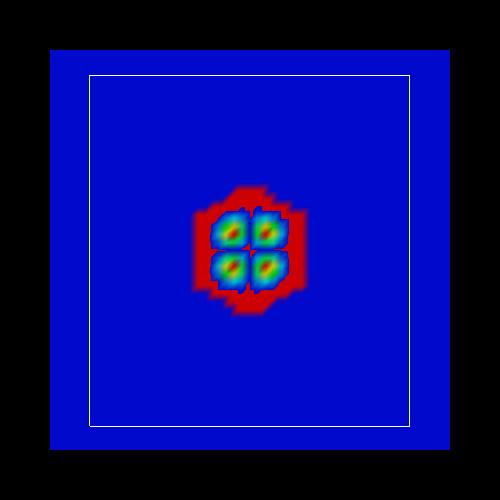
Figure 2.4.8.46 Probability density \(\Psi^2\) of the \(6^\mathrm{th}\) electron state in the QD.
Version of this tutorial for nextnano³ can be found here .
Last update: 11/07/2024